
Although Samsung recently outperformed TSMC in the quest to develop the most cutting-edge chips ever, TSMC is the unchallenged leader in the contract chip manufacturing sector. Even while the startup still has a lot to prove if it hopes to win over TSMC’s loyal clients, it now has a possibility of landing additional significant chip contracts.
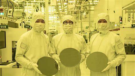
At its Hwaseong facility, Samsung has formally begun chip mass production using a 3nm process node with gate-all-around transistors. In the process, the Korean tech giant defeated competitor TSMC in the battle to create cutting-edge manufacturing processes for the rising performance and energy-efficiency requirements of the hardware sector.
When compared to its own 5nm node, the business claims the new manufacturing technique provides considerable benefits, including a 45 percent increase in power efficiency, a 16 percent decrease in area, and a performance boost of up to 23 percent.
Currently in development is a second-generation 3nm technology that will cut down power use and area size by 50% and 30%, respectively. There should be a 30% gain in performance as well, however yield and other crucial information are unknown.
According to the business, the development of high-performance and specialized low-power computing applications would be the main emphasis of its existing 3nm capacity. Later, it will extend to mobile chipsets, an area where Samsung recently ran into some yield problems. It’s unclear at this time if this will take place before or after the company moves 3nm manufacturing to its new Pyeongtaek site.
To read our blog on “Samsung is reported to be raising chip prices by 20%,” click here.